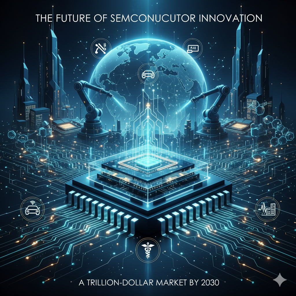
Executive summary
The semiconductor industry is entering a new era defined less by single-die transistor scaling and more by system-level innovation: new transistor architectures, higher-precision lithography, advanced packaging and heterogeneous integration, photonics and co-packaged optics, and the rapid commercialization of specialized AI and HPC fabrics. These changes are reshaping value chains, relocating capital, and creating fresh strategic choices for device makers, foundries, OSATs, and system integrators. Unity Innovate’s perspective: companies that combine deep process capability with systems thinking and that invest in partner ecosystems, advanced packaging, and software–hardware co-design will capture the disproportionate value of the next decade.
- Macro trends shaping the near future
1.1 From transistor count to system performance
Process node naming (7 nm, 5 nm, 3 nm, 2 nm) remains important, but its competitive value increasingly derives from how process advances are combined with packaging, chiplets, and co-design to deliver system performance (latency, throughput, power efficiency) rather than raw transistor density alone. Leading foundries are already preparing for nanosheet / GAA transistor architectures that promise step-changes in energy efficiency and performance per watt a foundational enabler for next-generation HPC and mobile SoCs.
1.2 Lithography: enabling the angstrom era
High-NA Extreme Ultraviolet (EUV) lithography is moving from R&D into manufacturing proof points. High-NA EUV systems extend patterning capability and are a gate-opener for the most advanced nodes and for tighter, more complex interconnect geometries. This allows device makers to push transistor scaling and pattern precision further while improving yield trajectories on new architectures.
1.3 Packaging, chiplets and heterogeneous integration
The semiconductor value pool is shifting upward into advanced packaging: 2.5D interposers, 3D stacking, fan-out wafer-level packages, and chiplet ecosystems. For AI, telecom and edge compute workloads, heterogeneous integration (combining logic, memory, photonics, power and sensors in a single package) is now the fastest route to higher system performance without incurring the full cost and complexity of further node scaling. This packaging pivot is a defining commercial lever for differentiated silicon platforms.
1.4 Photonics, optics and the co-packaged future
Optical connectivity, silicon photonics and co-packaged optics is moving from niche into mainstream for data centers and high-bandwidth links. Photonics integration reduces electrical I/O bottlenecks and energy per bit, enabling denser and more energy-efficient AI fabrics and telecom systems. Market forecasts and recent platform launches indicate accelerating demand for integrated photonics over the next 3–5 years.
1.5 Manufacturing footprint & maturity nodes
While advanced nodes receive the limelight, strategic shifts are happening across wafer sizes and mature nodes: fabs are being modernized and capacity reallocated (e.g., phasing out older 6-inch lines), and investments are being concentrated in 12-inch fabs and advanced facilities. These moves affect supplier strategies, OSAT capacity planning, and regional policy decisions.
2. Latest technical innovations worth watching
2.1 Gate-All-Around (GAA) and nanosheet transistors
GAA / nanosheet transistors replace FinFET geometries at the most advanced nodes and provide better electrostatic control and energy efficiency essential for delivering higher performance at lower power for AI and mobile SoCs. Several leading fabs are in risk production or ramping these architectures as part of their 2 nm roadmap.
2.2 High-NA EUV enabling finer pitch patterning
High-numerical-aperture EUV tools improve resolution for the most critical layers. These machines are complex and costly, but their deployment is a linchpin for continued transistor scaling and advanced interconnect geometries. Early shipments and collaborative lab programs have accelerated path-to-production learning.
2.3 Advanced packaging & chiplet ecosystems
Chiplets + advanced interposers let designers mix best-of-breed IP (compute dies from different processes, HBM stacks, analog/RF subsystems, photonics) into scalable, modular systems. OSATs and foundries are offering packaging platforms and silicon photonics co-integration to shorten time-to-market for AI accelerators and network platforms. Expect more standardization efforts and ecosystem marketplaces for interoperable chiplets.
2.4 Silicon photonics and co-packaged optics
Silicon photonics platforms are maturing for 200G+ per channel links; integration at the package level reduces latency and power for data center switches and accelerators. Start-ups and incumbents are converging on CMOS-compatible photonic building blocks, enabling broader adoption across cloud and telecom infrastructure.
2.5 Materials, packaging chemistry and reliability advances
From novel interconnect metallurgies to low-k dielectrics and thermal interface materials, ongoing materials innovations improve signal integrity and thermal management in 3D stacks. These incremental materials advances frequently unlock packaging density and long-term reliability for stacked die configurations.
3. Industry & supply-chain implications
3.1 Value capture shifts toward systems and packaging
Profit pools will increasingly favour companies that can deliver system-level differentiation: vendors able to provide packaged sub-systems (chip + memory + photonics + thermal solution + software) will command premium margins over commodity logic ramps.
3.2 Capital intensity and regionalization
The move to advanced nodes and new lithography tools drives enormous capital requirements and ties into geopolitical incentives. Policy instruments (e.g., CHIPS acts) and national incentives are shaping where capacity is built and how supply chains localize critical steps.
3.3 Talent and cross-discipline skills
Success requires talent combinations that span materials science, device physics, packaging engineering, and systems software. Organizations should invest in cross-functional programs and partnerships with research institutes to accelerate learning curves.
Strategic recommendations for industry players
For Foundries & IDMs
- Invest in mixed-signal, photonics, and packaging roadmaps alongside node development. High-NA EUV and GAA will matter but so will your packaging offer.
- Develop chiplet interfaces and standards (power, thermal, interposer protocols) to attract multi-customer ecosystems.
For OSATs & Packaging Specialists
Scale 2.5D/3D integration capability and strengthen partnerships with silicon photonics providers. Offer validated reference designs and thermal/IP protection services.
For System OEMs & Cloud Providers
Adopt co-design procurement models: procure silicon and packaging together with joint roadmaps (e.g., co-optimization of interposer routing with accelerator architecture) to maximize system energy efficiency.
How can we help you?
- Roadmap synthesis & scenario planning: Align R&D, capital and M&A plans with multiple node-and-package futures.
- Ecosystem mapping & partner selection: Identify ideal OSAT, IP and photonics partners for co-development.
- Go-to-market & product definition: Help system OEMs convert packaging and co-design advantages into customer value propositions.
- Pilot line & testbed strategy: Design pilot programs to derisk High-NA and 3D stacking trials before full capital commitment.
The semiconductor industry’s next decade will be a story of integration over isolation: new transistor physics (GAA), enabling lithography (High-NA EUV), and the sudden commercial relevance of packaging, photonics, and chiplets. For strategy teams, the imperative is clear think in systems, not isolated nodes. Companies that combine process excellence with packaging leadership, ecosystem orchestration, and software–hardware co-design will define winners in the coming wave of innovation.